


It’s nonetheless a particularly difficult proposition. “Packaging isn’t as straightforward as saying, ‘I wish to run 100,000 wafers per 30 days,’” says Jim McGregor, a longtime chip trade analyst and the founding father of Tirias Analysis, referring to a steady stream of chips in varied levels of manufacturing. “It actually comes down as to whether Intel’s [packaging] fabs could make offers. If we see them increasing these operations extra, that’s an indicator that they’ve.”
Final month, Anwar Ibrahim, the prime minister of Malaysia, revealed in a put up on Fb that Intel is increasing its Malaysian chip-making services, which have been first established again within the Seventies. Ibrahim mentioned the pinnacle of Intel’s Foundry, Naga Chandrasekaran, had “outlined plans to begin the primary section” of enlargement, which would come with superior packaging.
“I welcome Intel’s choice to start operations for the complicated later this 12 months,” a translated model of Ibrahim’s put up learn. An Intel spokesperson, John Hipsher, confirmed that it’s constructing out extra chip meeting and check capability in Penang, “amid rising international demand for Intel Foundry packaging options.”
Bundle Retailer
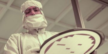
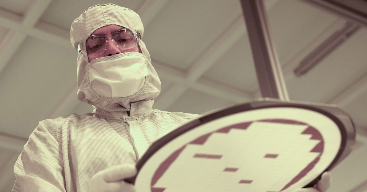
In response to Chandrasekaran, who took over Intel’s Foundry operations in 2025 and spoke solely with WIRED throughout the reporting of this story, the time period “superior packaging” itself didn’t exist a decade in the past.
Chips have all the time required some form of integration of transistors and capacitors, which management and retailer vitality. For a very long time the semiconductor trade was centered on miniaturization, or, shrinking the dimensions of parts on chips. Because the world started demanding extra from its computer systems within the 2010s, chips began to get much more dense with processing items, high-bandwidth reminiscence, and the entire crucial connective components. Ultimately, chipmakers began to take a system-in-packages or package-on-package strategy, by which a number of parts have been stacked on high of each other as a way to squeeze extra energy and reminiscence out of the identical floor area. 2D stacking gave approach to 3D stacking.
TSMC, the world’s main semiconductor producer, started providing packaging applied sciences like CoWoS (chip on wafer on substrate) and, later, SoIC (system on built-in chip) to clients. Primarily, the pitch was that TSMC would deal with not simply the entrance finish of chip-making—the wafer half—but in addition the again finish, the place the entire chip tech could be packaged collectively.
Intel had ceded its chip manufacturing result in TSMC at this level, however continued to spend money on packaging. In 2017 it launched a course of known as EMIB, or embedded multi-die interconnect bridge, which was distinctive as a result of it shrunk the precise connections, or bridges, between the parts within the chip package deal. In 2019, it launched Foveros, a complicated die-stacking course of. The corporate’s subsequent packaging development was an even bigger leap: EMIB-T.
Introduced final Could, EMIB-T guarantees to enhance energy effectivity and sign integrity between all of the parts on the chips. One former Intel worker with direct data of the corporate’s packaging efforts tells WIRED that Intel’s EMIB and EMIB-T are designed to be a extra “surgical” method of packaging chips than TSMC’s strategy. Like most chip developments, that is presupposed to be extra energy environment friendly, save area, and, ideally, save clients cash within the lengthy runThe firm says EMIB-T will roll out in fabs this 12 months.


